Keynote Speakers
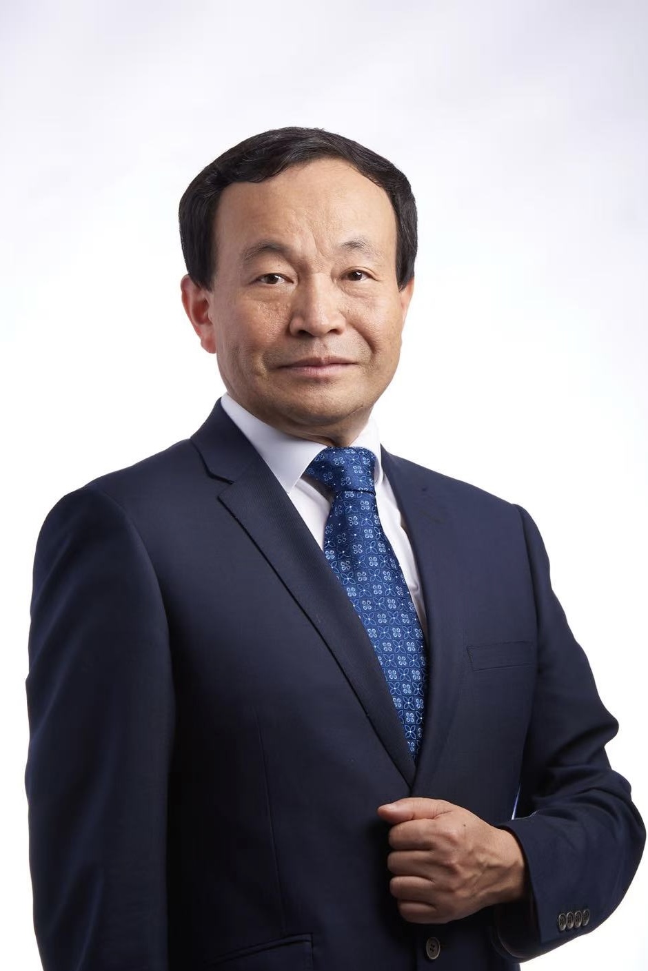
| Dapeng YuInternational Quantum Academy, China Prof. Dapeng Yu, Academician of the Chinese Academy of Sciences and Fellow of the American Physical Society (APS), is currently a professor at the School of Physics, Peking University, and the president of the Shenzhen International Quantum Academy. He also serves as the chairman of the Quantum Information Society of the Chinese Institute of Electronics. He has long been engaged in research on quantum computing, quantum state control of condensed matter, and the development of key core scientific instruments in the field of quantum information. In recent years, Prof. Yu’s main research has focused on the precise quantum control of quantum phases of matter, achieving a series of significant research results with substantial international impact and making major breakthroughs in the independent development of several scientific instruments. Speech Title: Everything is Quantizable:Quantum Computing is Everyone’s Responsibility Abstract: Quantum mechanics describes the most fundamental layer of physical reality—the set of rules governing how everything in the universe behaves. In that sense, at its core, "everything is quantum." Quantum computing is the ambitious endeavor to harness these rules, representing one of the most demanding engineering challenges of our time. It pushes the boundaries of our ability to control the microscopic world and could ultimately unleash the disruptive computational power needed to drive the next industrial revolution. As the saying goes, "Every craftsperson needs the right tools." This report begins with a brief introduction to the Shenzhen International Quantum Institute. It then turns to the current state of the quantum information industry, both in China and globally, and underscores why scientific instrumentation, self-reliance, and independent R&D are critical to success in this field. |
| Wei HongSoutheast University, China Wei Hong received the B.S. degree from the University of Information Engineering, Zhengzhou, China, in 1982, and the M.S. and PhD degrees from Southeast University, Nanjing, China, in 1985 and 1988, respectively, all in radio engineering. He is currently a professor of the School of Information Science and Engineering, Southeast University. In 1993, 1995, 1996, 1997 and 1998, he was a short-term visiting scholar with the University of California at Berkeley and at Santa Cruz, respectively. He has been engaged in numerical methods for electromagnetic problems, millimeter wave and terahertz theory and technology, antennas, RF technology for wireless communications etc. He has authored and co-authored over 400 technical publications and 5 books. He twice awarded the National Natural Prizes of China, once awarded the National Science and Technology Progress Award, four times awarded the first-class Science and Technology Progress Prizes issued by the Ministry of Education of China and Jiangsu Province Government, and 2021 IEEE MTT-S Microwave Prize etc. Dr. Hong is a Fellow of IEEE, Fellow of CIE, the vice presidents of the CIE Microwave Society and Antenna Society, and was an elected IEEE MTT-S AdCom Member during 2014-2016, served as the Associate Editor of the IEEE Trans. on MTT from 2007 to 2010. Speech Title: Research Progress in Terahertz Devices, Chips, and Systems Abstract: In this talk, the recent research progress in terahertz (THz) devices, chips and systems in the State Key Laboratory of Millimeter Waves (SKLMMW) of Southeast University and cooperative enterprises are reviewed. |
 | Tianchun YeUniversity of Chinese Academy of Sciences, China Tianchun Ye, born in 1965, he is an IEEE Fellow and a graduate of the Department of Electronic Engineering at Fudan University. He previously served as the Director of the Institute of Microelectronics, Chinese Academy of Sciences, and led a National Science and Technology Major Project. He has received three National Technology Invention Awards and four First-Class Invention Awards at the ministerial and provincial levels. Leading his team in over a decade of persistent research, he proposed a series of innovative technical methodologies and achieved multiple major inventions at the forefront of international standards. These technologies have been adopted by leading enterprises both in China and abroad for the mass production of cutting-edge products, making pioneering contributions to the self-reliance and development of China's advanced integrated circuit processes. Speech Title: Technology Innovation in Integrated Circuit Transistor Process Abstract: Integrated circuit process evolution is the fundamental basis for the development of modern information and artificial intelligence technologies. Over the past few decades, China has been making continuous efforts in this field. Starting from the 90nm node, integrated circuit CMOS transistors have demanded the development of new processes, materials, and structures to overcome key bottlenecks in PPA scaling by generations. The Institute of Microelectronics of the Chinese Academy of Sciences (IMECAS) has long been engaged in the research and development of innovative transistor technologies. They have made a great breakthrough on technical challenges such as precise gate control, transistor performance modulation, and structural scaling in both 22nm high-k/metal gate-last, 14nm FinFET, and up-to-date GAA transistor processes, established a technical system with comprehensive independent intellectual property rights, and successfully applied it to domestic and international cutting-edge integrated circuit products. |
 | Tian-ling RenTsinghua University, China Prof. Tian-Ling Ren is a distinguished professor at Tsinghua University. He serves as Vice Dean of the School of Information Science and Technology, and Director of the Tsinghua University-BEIGC Joint Research Center. He is IEEE Fellow, and Chinese Society of Micro-Nano Technology Fellow. His research focuses on intelligent micro-nano electronic devices, 2D nanoelectronic devices, flexible wearable systems, and intelligent sensing chips. He has led many national key research projects and achieved world-renowned innovations, including the world’s shortest gate-length transistor, the first graphene intelligent artificial throat, high-performance flexible AI chips, and intelligent healthcare systems. He has published over 900 papers in top journals and conferences, such as Nature and IEDM, with more than 30,000 Google Scholar citations. He holds more than 200 patents and has been selected as an Elsevier Highly Cited Researcher for consecutive years. Speech Title: Novel Device and Chip Technologies Driving Moore’s Law Abstract: As Moore’s Law faces severe physical bottlenecks—including thermal and quantum mechanical limits—sustaining the exponential growth of integrated circuits requires innovations beyond simple dimensional scaling. This talk presents recent advances in novel device and chip technologies that both extend and go beyond Moore’s Law. In the extending direction, we demonstrate a sub-1nm gate-length transistor with a physical gate length of only 0.34 nm using a graphene edge gate and a MoS₂ channel, pushing device scaling to the atomic limit. We also introduce flexible in memory computing chips that achieve high clock frequency and energy efficiency, enabling edge computing on conformable substrates. In the beyond Moore direction, we highlight smart graphene based artificial throats that restore voice communication for laryngectomees, and a motion artifact free 12 lead dynamic ECG system with on chip AI processing for unobtrusive, continuous cardiac monitoring. These developments illustrate that novel devices enabled by low dimensional materials and flexible electronics can effectively promote Moore’s Law with wide intelligent healthcare and human machine interface applications. |

FET100 Speakers
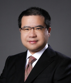 | Han WangUniversity of Hong Kong, China Han Wang is a Professor in the Department of Electrical and Computer Engineering at the University of Hong Kong (HKU). He also serves as the Director of HKU Center for Advanced Semiconductors and Integrated Circuits and Co-Director of the Institute of Mind at HKU. Prior to joining HKU, he was tenured Associate Professor at the University of Southern California. In 2021-2023, he served as the Head of New Material and Device Research department at Taiwan Semiconductor Manufacturing Company (TSMC), concurrent to his faculty appointment. He has also served as the Chair of the IEEE EDS Neuromorphics Technical Committee and Chair of the IEEE ED/SSC Hong Kong Joint Chapter.His work has been recognized with numerous prestigious awards including the IEEE IEDM Roger A. Haken Best Paper Award, US NSF CAREER Award, IEEE Nanotechnology Council Early Career Award, the US Army Research Office Young Investigator Award. He is the IEEE Nanotechnology Council Distinguished Lecturer and the Clarivate Highly Cited Researcher for eight consecutive years 2018-2025. Prof. Wang is a Fellow of IEEE. Speech Title: CMOS Technology in the Nanoscale Era Abstract: This talk provides an overview of the evolution of CMOS technology, tracing its remarkable journey from the early logic gates of the 1970s to today’s advanced nodes and beyond. The first part reviews key historical milestones—including the scaling principles of Dennard and Moore, the transition from planar to FinFET devices, and the introduction of strain engineering, and high k/metal gates—that have sustained performance and density gains over five decades. The second part focuses on future development directions for advanced-node CMOS. It examines emerging device architectures such as nanosheet GAAFETs, forksheet FETs, and CFETs, along with novel channel materials (2D semiconductors, Ge, etc.). On the integration front, the talk discusses monolithic and hybrid 3D integration and backside power delivery networks. Challenges related to power density, variability, interconnect delay, and lithography extensibility will be highlighted. The talk concludes with a forward looking perspective on how emerging technologies will shape the next decade of CMOS innovation. |
| Pui-In MakUniversity of Macau, China Pui-In Mak is Chair Professor at the University of Macau, Macau, China, Director of the State-Key Laboratory of Analog and Mixed-Signal VLSI, and Director of the Guangdong-Macao Joint Laboratory for Modular Chip Design and Testing. His research interests are on analog and radio-frequency circuits and systems for wireless and multidisciplinary innovations. He received the Xplorer Prize in 2022, and is recognized as one of the Top Contributing Authors of ISSCC at its 70th anniversary in 2023, and the Medal of Merit-Education from the Macau government in 2024. He is currently AdCom Member of the IEEE Solid-State Circuits Society and Editor-in-Chief of the IEEE Solid-State Circuits Letters, and was an Associate Editor of the IEEE Journal of Solid-State Circuits. He is a Changjiang Scholar, Overseas Expert of the Chinese Academy of Sciences, Fellow of the IEEE, IET and UK Royal Society of Chemistry. He is a foreign academician of the Academy of Sciences of Lisbon (ACL), Portugal. Speech Title: The Frontiers of Microelectronic Engineering over the Next Decade Abstract: This talk explores the transformative landscape of microelectronic engineering over the next decade. As we navigate advancements in integrated circuits (IC) with artificial intelligence (AI), we will highlight emerging trends that promise to redefine the experience of humans interact with their surroundings that will be collectively proactive, and highly personalized. Key topics will include the embodiment of power-efficient edge AI chips in wearables/robots, ultra-low-power radio chips for battery-free wireless connectivity, and easy-to-use advanced instruments, shifting towards a highly-efficient healthcare home system. By examining the current challenges and opportunities of IC+AI, this presentation aims to envision a future where microelectronics plays a pivotal role in re-shaping our quality of life. Join us as we delve into the frontiers that will surf on the next big wave of engineering breakthroughs. |
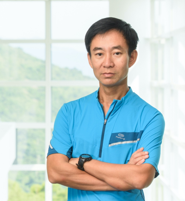 | Mansun ChanThe Hong Kong University of Science and Technology, China Dr. Mansun Chan is the Alex Wong Siu Wah Gigi Wong Fook Chi Professor of Engineering and Chair Professor in the Department of Electronic and Computer Engineering at the Hong Kong University of Science and Technology. He received his Ph.D. degree from the University of California, Berkeley. As an internationally recognized leader in semiconductor devices and compact modeling, he has authored over 350 journal papers and 500 conference papers. He is best known for his pivotal contributions to the unified BSIM compact model for SPICE, which became the first widely adopted industrial standard MOSFET model, and for leading the first demonstration of stacked CFET technology to extend CMOS scaling beyond the 2‑nm node. Beyond research, Prof. Chan has played a major role in technology leadership and professional education. He is an IEEE Fellow and Distinguished Lecturer, has served in multiple leadership roles within the IEEE Electron Device Society, and has been deeply involved in advancing engineering education through large‑scale online courses, outreach programs, and industry engagement. He is also active in entrepreneurship, having co‑founded and invested in numerous technology startups. Speech Title: The Role of Compact Modeling in Bridging Conceptual Understanding and Production in CMOS Technology Abstract: This talk reviews the historical role of compact modeling in enabling CMOS technology from academic research to industrial production. It begins with the development of SPICE as an academic circuit simulator and the early Meyer model, which supported initial MOS circuit analysis. As CMOS scaled, compact models evolved toward standardization, with BSIM3 becoming the first widely adopted industrial standard. The talk contrasts academic and industrial modeling requirements and shows how compact models actively guided technology development and manufacturing. Finally, it discusses the continuing importance of parameter extraction and physics‑based modeling methodologies in the emerging AI‑driven modeling era. |
Tutorial invited Speakers
| Kong-Pang PUNDepartment of Electronic Engineering, The Chinese University of Hong Kong, China Prof. Kong-pang Pun received his B.Eng. and M.Phil. degrees in Electronic Engineering from the Chinese University of Hong Kong (CUHK) and his Ph.D. degree in Electrical and Computer Engineering from the Instituto Superior Técnico, University of Lisbon, Portugal. He is currently a full professor in the Department of Electronic Engineering at CUHK. Prof. Pun was the General Co-Chair and Technical Program co-chair of the IEEE EDSSC in 2008 and 2016, respectively, among his other services. Prof. Pun’s expertise includes high power-efficiency integrated circuits for data conversion and natural signal interface. He has published over 200 peer-reviewed journal and conference papers and co-authored two books in the area of CMOS integrated circuits design. He pioneered the field of N-path filter-based bandpass Delta-Sigma modulators. SpeechTitle: Design of Bandpass Delta-Sigma Modulators Based on N-path Filters Abstract: Bandpass delta-sigma modulators (BP-DSMs) are specialized analog-to-digital converters (ADCs) designed to digitize narrowband signals centered at high frequencies, such as intermediate or radio frequencies. They find unique applications in digital radio receivers, software-defined radio, radar and sonar systems, and medical ultrasound imaging by offering critical benefits like the elimination of analog mixers, exceptional narrowband resolution, and frequency programmability. Traditionally, BP-DSM loop filters are implemented using active-RC, Gm-LC, or Gm-C circuits. However, as power efficiency and integration demands increase, a new class of BP-DSMs based on switched-RC N-path filters (NPFs) has emerged. Compared to conventional approaches, NPF-based BP-DSMs offer better compatibility with advanced CMOS processes, superior power efficiency, and wider center-frequency programmability for narrowband signals. This tutorial will walk attendees through the architectural design and practical circuit implementation of the NPF-based BP-DSM with design examples, concluding with a perspective on the future of this technology. |
| Min ZhangThe Chinese University of Hong Kong, Shenzhen, China Min Zhang is a Professor and Presidential Fellow of the School of Science and Engineering at the Chinese University of Hong Kong, Shenzhen. She received her bachelor and master degrees from Xi’an Jiaotong University and her Ph.D. degree from the Department of Electronic and Computer Engineering at Hong Kong University of Science and Technology. She held academic and industrial positions at Solomon Systech Limited (Hong Kong), Peking University, and Hong Kong Applied Science and Technology Research Institute from 2006 to 2024. Her research interests focus on emerging microelectronic devices, including flexible and stretchable electronics, neuromorphic electronics, nanoelectronics, bioelectronics, and advanced displays. She has published over 160 peer-reviewed papers and 4 book chapters, and has been authorized with more than 20 patents. She has been invited to deliver tutorials and invited talks at more than 30 renowned international conferences. She is a senior member of IEEE, an associate editor of IEEE Open Journal on Immersive Displays, a technical committee member of SID Beijing Branch. She has served as technical program chairs/committees and organizing chairs/committees in numerous conferences, and reviewers for numerous prestigious journals. Speech Title: Flexible and stretchable thin-film transistors: From Advanced Materials to Neuromorphic Applications Abstract:Flexible and stretchable electronics have garnered intense interest due to their transformative potential for emerging applications, ranging from imperceptible wearable devices and skin prosthesis repair to soft robotic perceptions and conformable human-machine interfaces. However, the field continues to face challenging obstacles, including material self-limiting fabrication, the trade-off between mechanical flexibility and electrical performance, and the need for stable large-area integration. Nanocarbon based electronics is of great promise to solve these problems for their intrinsic flexibility or stretchability, high carrier mobility, and capability to synthesize as semiconducting or metallic. At the same time, the landscape of flexible thin-film transistors (TFTs) has significantly expanded to include high-performance metal oxide semiconductors, specifically Indium Gallium Zinc Oxide (IGZO), and flexible silicon technologies. These materials provide complementary advantages in terms of CMOS, mobility, uniformity, and compatibility with established fabrication processes. Beyond logic and control circuits, a pivotal frontier in this domain is the development of TFT-based synaptic transistors, which mimic biological plasticity to enable hardware-level neuromorphic computing and artificial intelligence at the edge. This tutorial will provide a comprehensive overview of the state-of-the-art in flexible and stretchable TFTs. We will examine the device physics, fabrication mechanisms, and circuit integration of carbon nanotube, IGZO, and flexible silicon-based active layers. Special emphasis will be placed on the design and operation of synaptic transistors for neuromorphic applications, as well as strategies for future system integration. By bridging the gap between novel semiconductor materials and bio-inspired computing architectures, this session aims to propose versatile solutions for the next generation of intelligent, soft electronic systems. |
| Lining ZhangPeking University,China Lining Zhang is an Assistant Professor in the School of Electronic and Computer Engineering at Peking University, Shenzhen. He received his Ph.D. from the Hong Kong University of Science and Technology. His research focuses on model-driven next-generation computing systems, advanced electronic design automation (EDA), neuromorphic computing, and novel logic and memory devices. Speech Title: Accelerating Device Modeling and Design-Technology Co-Optimization with AI Algorithms Abstract: In the post-Moore era, Design-Technology Co-Optimization (DTCO) is indispensable for meeting advanced power, performance, and area (PPA) requirements. However, traditional physics-based compact models suffer from explosive parameter growth and lengthy development cycles. This tutorial introduces modern Machine Learning-based Device Modeling (MLDM) as an agile and highly accurate alternative. It presents the innovative PHIMO-NN framework, which bridges device physics and artificial neural networks. By embedding tiny neural networks into a physical backbone, PHIMO-NN successfully captures complex short-channel and mobility degradation effects while maintaining strict physical consistency and robust extrapolation capabilities. Fully implemented in Verilog-A, this framework reduces parameter complexity by over 70% and significantly accelerates circuit simulation workflows compared to conventional BSIM models. Finally, the tutorial highlights the open-source Peking University Predictive PDK (PKP), showcasing how it enables standard-cell and end-to-end DTCO pathfinding for advanced nanosheet Gate-All-Around (GAA) architectures. |


Invited Speakers
| Yang ChaiThe Hong Kong Polytechnic University, Hong Kong, China Prof. Yang Chai is the Chair Professor of Semiconductor Physics of the Hong Kong Polytechnic University. He is an IEEE Distinguished Lecturer, an IEEE Fellow, an Optica Fellow, IOP Fellow, and AAIA Fellow. He is the Director of Research Institute for Artificial Intelligence of Things, the Director of Joint Research Center of Microelectronics, and the Associate Dean of Faculty of Science (Research) at the Hong Kong Polytechnic University. He is also the Chair of Semiconductor Nanotechnology Alliance, the Vice President of the Physical Society of Hong Kong, and an Associate Editor of ACS Nano. He is a receipt of the Falling Walls Science Breakthroughs in Engineering and Technology for his work on “Breaking the Wall of Efficient Sensory AI Systems”, the BOCHK Science and Technology Innovation Prize in the field of AI and Robotics, The Croucher Senior Fellowship, The Ho Leung Ho Lee Foundation Science and Technology Innovation Award, and NSFC Distinguished Scholar. His current research interest mainly focuses on emerging electronic devices. Speech Title: Bioinspired In-Sensor Computing for Artificial Vision Abstract: The demand for accurate perception of the physical world leads to a dramatic increase in sensory nodes. However, the transmission of massive and unstructured sensory data from sensors to computing units poses great challenges in terms of power‐efficiency, transmission bandwidth, data storage, time latency, and security. To efficiently process massive sensory data, it is crucial to achieve data compression and structuring at the sensory terminals. In‐sensor computing integrates perception, memory, and processing functions within sensors, enabling sensory terminals to perform data compression and data structuring. We will overview optoelectronic intelligence for bioinspired in-sensor computing in artificial vision. We will examine optoelectronic devices that can compress and structure multidimensional vision information, and demonstrate a few vision sensors for different scenarios, including visual adaptation, motion perception, as well as event-driven vision sensors for spiking neural network. |
 | Yeliang WANGBeijing Institute of Technology,China Dr.Yeliang Wang is a full professor and the Dean in School of Integrated Circuits and Electronics, Beijing Institute of Technology. He received his B.S. and M.S. degree from the Wuhan University of Technology, Ph.D. degree from Institute of Physics(IoP), Chinese Academy of Sciences (CAS). He then joined in the Max-Planck-Institute for Solid Research, Germany as a Humboldt Fellow (hosted by Prof. Klaus Kern). He was appointed an associate professor in 2008 and a full professor in 2013 in the IoP, CAS. He set up a research group in Beijing Institute of Technology (BIT) in 2018. He was awarded as the National Science Fund of China for Distinguished Young Scholars. His current research interest is the controlled growth, quantum properties and funtional nanodevices of novel two-dimensional materials and heterostructures. He held more than 310 papers published on high-profile journals. Speech Title: Tunning Properties of Novel 2D Heterostructures & Devices Abstract: The novel properties of graphene honeycomb structure have spurred tremendous interest in investigating other two-dimensional (2D) layered structures beyond graphene for nanodevices. In this talk, I will mentioned the fabrication and properties of several 2D materials such as magnetic VSe2 monolayer, semiconducting PtSe2 monolayer, charge density wave NbSe2 superstructure and related heterostructures and devices, as well as quantum properties for nanoelectronics and valleytronics will also be introduced. In addition, the stacking heterolayers for ultrahigh denisty information storage, Majorana bound states and quantum computing will be also presented. Complex micro-nano architectures with high spatial resolution and tunable depth profiles are also realized by new lithography technique.The precise structural configurations at atomic-resolution of these materials and device transport properties will also be introduced. |
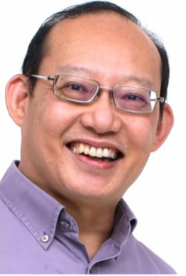 | Cher Ming TanChang Gung University, Taiwan Professor Cher Ming Tan is a leading authority in reliability engineering, currently serving as a Professor at Chang Gung University (Taiwan) and Director of the Reliability Science and Technology Center. Since 2024, he has also held the presidency of the Taiwan Reliability Technology Promotion Association. His career began in 1984 at Fairchild Semiconductor, followed by pivotal roles at Hewlett-Packard and Chartered Semiconductor, which built his cross-disciplinary expertise in materials, devices, and system-level reliability before he transitioned to academia in 1996. Professor Tan is a Senior Member of IEEE and a Fellow of several prestigious institutions, including the Singapore Quality Institute, Institute of Engineers, Singapore and the International Association of Advanced Materials, Swedan. He is a contributor to international standards like IEEE 1624 and IEEE 1413. Since 2007, he has served as an IEEE EDS Distinguished Lecturer, delivering over 40 keynote addresses and providing systematic reliability training at major conferences such as IRPS, RAMS, and EDTM. He has Published over 400 papers in high-impact journals and authored 14 books on reliability, with his work on Simulated Annealing exceeding 60,000 downloads. He is recognized among Stanford University’s Top 2% Scientists worldwide, specifically ranking in the top 0.043% for Semiconductor Reliability. He also provided expert consulting to more than 50 international organizations, including NASA, TSMC, Microsoft, the Taiwan Space Agency, and Aptiv. Speech Title: A Multi-Physics Toolkit for Predictive Electromigration Modeling in Advanced IC Interconnections Abstract: As semiconductor technologies advance toward complex chiplet integration and extreme miniaturization, the reliability of integrated circuit (IC) interconnections has emerged as a primary bottleneck for system performance. High current densities in these scaled interconnects make electromigration (EM) a critical failure mechanism. However, traditional assessment methods, such as Black’s Equation, are increasingly inadequate; they lack the capability to localize void-nucleation sites or effectively couple the complex 3D multi-physics driving forces—specifically thermal and thermo-mechanical stress gradients—present in realistic structures. This talk introduces an advanced simulation toolkit developed as an Ansys Customization Toolkit designed for the rapid and accurate assessment of interconnect reliability. By utilizing a dynamic Atomic Flux Divergence (AFD) formulation derived from the first principles of thermodynamics, the toolkit captures the spatial-temporal evolution of EM-induced degradation. A key innovation of this toolkit is its integration of microscale defect dynamics and energy barriers—parameters often experimentally inaccessible—computed via Density-Functional Theory (DFT) and Finite-Element Analysis (FEA). This enables the modeling of synergistic effects between electron-wind, thermal gradients, and stress-migration in a full 3D environment. With such ab-initio modeling, strong correlation between estimated failure times and experimental data, achieving low error rates for Copper (0.37%) and Aluminum (0.27%) interconnects are observed. This toolkit can facilitate the evaluation of novel materials, barrier metals, and layouts before committing to resource-intensive back-end-of-line (BEOL) process development. By providing a robust predictive framework, this toolkit serves as a vital tool for optimizing reliability and accelerating the development cycle of advanced integrated systems. |
| Mohammad SAMIZADEH NIKOONanyang Technological University, Singapore Mohammad Samizadeh Nikoo is a Nanyang Assistant Professor in the School of Electrical and Electronic Engineering (EEE) at Nanyang Technological University (NTU), Singapore. He is the founding director of the Innovative Electronic & Electromagnetic Device Laboratory (i–Lab). He received his PhD from EPFL, Switzerland, in 2022. In the same year, he joined the Integrated Systems Laboratory at ETH Zurich as a research scientist, before beginning his tenure-track appointment at NTU in 2023. Dr. Samizadeh Nikoo is a Fellow of the National Research Foundation, Singapore (Class of 2024). He has received several distinctions and awards and currently serves as the lead principal investigator (PI) on multiple national research projects. His research focuses on developing a new generation of high-frequency semiconductor components for future information technologies. Speech Title: High-Performance Electronic Metadevices for Millimeter-Wave and Terahertz Integrated Circuits Abstract: Approaching the terahertz band from the electronics side is of great technological importance, with the promise of advancing next-generation wireless communication systems toward 6G and beyond. However, inherent limitations of high-speed transistors, the primary building blocks of monolithically integrated high-frequency circuits, have hindered the realization of high-performance terahertz electronics. Electrical metastructures offer an alternative paradigm, in which modulation of the conductivity of a semiconducting layer controls collective quasi-electrostatic responses within a lumped structure, enabling electronic functionalities such as switching, mixing, and parametric amplification. Compared with conventional transistors, electrical metastructures enable ultra-low contact resistances, leading to record-high switching cutoff frequencies well beyond 10 THz in a compact device platform, referred to as electronic metadevices. The first part of this talk highlights recent advances in III-nitride electronic metadevices operating up to 1 THz and introduces a new generation based on quasi-one-dimensional electrical metastructures with enhanced electrical performance. We present theoretical insights into the collective responses governing the operation of electronic metadevices and elucidate their ultimate performance limits. In the second part, we introduce a metastructure-based paradigm for directly realizing high-performance millimeter-wave and terahertz components with ultracompact footprints, demonstrated the compatibility of metatronic devices with commercial silicon processes. |
| Eleni MAKARONAInstitute of Nanoscience and Nanotechnology, NCSR “Demokritos”, Greece Dr. Eleni Makarona is Director of Research at the Institute of Nanoscience and Nanotechnology, NCSR "Demokritos", Greece. She holds a PhD in Physics from Brown University (USA), where she trained under Prof. Arto V. Nurmikko on III-nitride optoelectronics, supported by a competitive graduate fellowship awarded to the top 10% of international applicants. Her research spans two parallel axes maintained continuously for nearly two decades: silicon photonic biosensors, and chemically synthesized metal oxide nanostructures. Her work on photonic sensors spans applications in biodiagnostics, food safety and quality assurance, and environmental monitoring. Moreover, she is co-inventor of the Broadband Mach-Zehnder Interferometer and Broadband Young Interferometer detection architectures — novel sensing principles that progressed from fundamental invention through patents to international prototype deployment. In metal oxide nanostructures, her work follows a material-first philosophy in which device concepts emerge from deep understanding of defect-driven mechanisms, spanning optoelectronics, sensing, energy harvesting, and hardware security. She has led or coordinated competitive research programs across European and national frameworks, and has delivered invited presentations at international conferences. She was awarded the Greek L'Oréal–UNESCO Award For Young Women in Science in 2010. Speech Title: Scalable Functional Devices Based on Chemically Synthesized ZnO Nanostructures: Bridging Synthesis and Device Functionality Abstract: Low-cost, chemically synthesized metal oxide nanostructures offer a compelling pathway toward scalable, cost-efficient, and sustainable electronic and sensing devices. However, building functional devices from such nanostructures requires more than mastering fabrication and compatibility with standard micro/nanofabrication processes — it demands a deeper understanding of the underlying physical mechanisms governing the material itself and of how these translate into, and ultimately dictate, device performance. This talk presents a device-oriented framework in which zinc oxide (ZnO) serves as a representative material platform. Central to this framework is the systematic investigation of defect-driven mechanisms emerging from the growth environment — mechanisms that, contrary to conventional device design assumptions, are shown to be the dominant determinants of functional behavior rather than structural geometry or intentional doping alone. This perspective enables the development of functional systems across diverse application domains. Representative implementations span ZnO-based homojunction devices, sensing platforms exploiting defect-mediated mechanisms, energy harvesting systems, and hardware security elements. Collectively, these demonstrate a coherent, fabrication-compatible, and scalable pathway for functional device realization from chemically synthesized nanostructures — one that redefines material imperfection not as a limitation to be suppressed, but as a design parameter to be understood, controlled, and exploited. |
 | Qianqian HuangPeking University, China Prof. Qianqian Huang is a Full Professor with Tenure in the School of Integrated Circuits at Peking University. Her research interests are in the area of emerging low-power devices for diverse applications, in particular tunnel devices and ferroelectric devices. She has authored/co-authored more than 100 technical papers in international journals and conferences and held more than 70 granted patents. She is the recipient of Chang Jiang Scholar (2023), the Chinese Young Women in Science Award (2022), Xplorer Prize (2020), IEEE EDS Early Career Award (2019), etc. Speech Title: Si Hybrid Tunnel FET-CMOS Foundry Platform for Ultra-low-Power Circuit Applications Abstract: This work demonstrates the recent progress on 55 nm Tunnel FET(TFET)-CMOS hybrid integration platform and its ultra-low-power circuit applications. By integrating the bulk-Si-based novel dopant-segregated TFET (DS-TFET) with large ION and record high ION/IOFF ratio, as well as the novel laminated isolation technology into the CMOS baseline technology, energy-efficient TFET-CMOS hybrid circuits are experimentally realized. 1Kbit TFET-Gated-Ground SRAM is implemented and demonstrated in MCU always-on domain showing sub-100nA ultra-low leakage, and a 6T hybrid TFET-CMOS SRAM-based digital CIM accelerator is designed showing high energy efficiency without performance or area penalty. Moreover, a novel DS-TFET-like device (AsyFET) with ultralow off-state leakage current and bidirectional conductivity is further demonstrated as the write transistor of 2T0C eDRAM, leading to the long retention of 3.9 s in 55nm technology node. The TFET-CMOS hybrid platform of this work demonstrates the great potential for cutting-edge power-dieting applications. |
 | Shurong DongZhejiang University, China Qiu Shi Distinguished Professor and director of Sensing and Micro-Integration Institute of Zhejiang University, Chief scientist of special project of the Ministry of Science and Technology, Military Strategic Expert Electronic field Committee, National Brain-Computer Interface Standards Committee, International PI of Cambridge University, One of the top 2% global scientists. He mainly engages in research on brain-machine interfaces and smart medical MEMS microsystem technologies. He has published 229 SCI papers, has an H-index of 48, and 6,809 citations on Google, 131 invention patents. Speech Title: Multimodal Integrated Neural Electrode Based on Flexible Electronics Abstract: Neural monitoring is a fundamental technology in neuroscience and neurological diseases. Multimodal neural monitoring can better observe neural and brain activity from multiple perspectives. How to integrate various observation techniques in a small area and meet the needs of different application scenarios is currently a challenge in the field of brain and neuroscience. This article introduces our team's recent work from implanted electrodes to wearable non-invasive electrodes, focusing on multimodal integrated neural electrode technology based on flexible electronics, so as to provide a reference for scientific research. |
 | Chao MaXi’an Jiaotong University, China Dr. Chao Ma is currently an Associate Professor and Ph.D. Supervisor at the School of Microelectronics, Xi’an Jiaotong University, and was selected for the XJTU Young Talent Support Plan. He received his Ph.D. degree in Electrical Engineering from Xi’an Jiaotong University in 2021, during which he was a visiting scholar at the University of California, Los Angeles (UCLA). After graduation, he conducted postdoctoral research at the School of Electronics, Peking University, as a “Boya” Postdoctoral Fellow. His research interests lie in high-performance pressure sensing and low-dimensional device integration, with a focus on: (1) AI-enabled tactile dexterous hands; (2) novel-principle sensing devices and electronic circuits, including (but not limited to) non-Hermitian electronic circuits; and (3) low-dimensional device integration for in-sensor computing. In recent years, he has published papers in leading journals, including Nature Electronics (front cover), Nature Communications, ACS Nano, and IEEE Electron Device Letters. He also holds five granted Chinese invention patents. Speech Title: Contact-dominated, field-enhanced flexible pressure sensors toward high-performance robotic skin Abstract: Motivated by the vision of functionalizing diverse human orientated future intelligent technologies with the ability to accurately and robustly detect various mechanical stimuli and interactions, intense efforts have been devoted to designing high-performance flexible pressure sensors, in particular for typical capacitive ones that feature low power consumption to support long-term continuous detection/monitoring. However, capacitive pressure sensors essentially suffer from limitations in terms of sensitivity, linearity, and working range. Here, we report a design strategy based on contact-dominated localized electric-displacement-field-enhanced capacitance and contact mechanics to dramatically improve the sensing response and linearity of capacitive sensors over a broad pressure range. We present a novel construction of integrated sensors by employing our contact-dominated design with floating-gate low-dimensional semiconductor transistors that enables the sensor to fully exploit the transistor’s on/off ratio range with enhanced sensing performance at a low operating voltage. Moreover, our sensor-equipped robotic arm demonstrates the potential to evaluate physical properties of fluids, and precisely and dynamically control to handle manipulation tasks. The proposed strategy can provide general design guidance for high-performance capacitive sensor, which would have a significant impact on human orientated future intelligent technologies. |
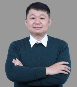 | Jiang Xu Hong Kong University of Science and Technology (Guangzhou), China Prof. Jiang Xu received his PhD from Princeton University and worked at Bell Labs, NEC Labs, and a startup company which is acquired by Qualcomm. He is the Founding Head of Microelectronics Thrust at Hong Kong University of Science and Technology (Guangzhou). Prof. Xu serves as the Associate Editor for IEEE TCAD and on the steering committees, organizing committees, and technical program committees of many international conferences, including OFC, DAC, DATE, ICCAD, CASES, CODES+ISSS, ASP-DAC, etc. Prof. Xu is awarded IEEE Computer Society Distinguished Contributor as the Charter Member in 2021. He was an IEEE Computer Society Distinguished Visitor and an ACM Distinguished Speaker. He authored and coauthored more than 180 book chapters and papers in peer-reviewed international journals and conferences. Prof. Xu and his students received Special Feature Award from ASP-DAC in 2026, Best Paper Award from the International Symposium on Memory Systems in 2023, IEEE Technical Committee on VLSI Best Paper Award of ISVLSI in 2018, and Best Poster Award from AMD Technical Forum and Exhibition in 2010. His research areas include AI system, electronic-photonic integration, power delivery and management, and hardware/software codesign. Speech Title: Breaking Interconnect Wall with Electronic-Photonic Integration Abstract: In the last 15 years, AI applications have required 4.3X more computation capacity every year, while Moore's Law can only offer 1.7X per year. AI systems are relying on not only advanced integration but also aggregation of growing numbers of GPU, CPU, accelerators and memories to meet the burgeoning performance requirements of AI applications under tight cost, energy, thermal, space, and weight constraints. However, interconnect technology develops slower than GPU, CPU and accelerators, and the gap is widening at 1.47X per year. This interconnect wall has become the major bottleneck of AI systems. Electronic-photonic integration piggybacks onto matured fabrication technologies to provide viable solutions to break the interconnect wall. Based on our decade-long quest to transform existing electronic computing systems with photonics, this talk will highlight our recent progress on electronic-photonic integration for aggregated systems. |
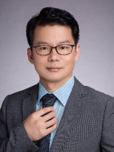 | Quan Pan Southern University of Science and Technology, China Quan Pan (Senior Member, IEEE) received his B.S degree in Electrical Engineering (EE) at University of Science and Technology of China (USTC) in 2005, and his Ph.D. degree in Electronics and Computer Engineering (ECE) at the Hong Kong University of Science and Technology (HKUST) in 2014. From 2014 to 2018, he was Senior Staff Engineer in one Silicon Valley startup company, working on 400GbE high-speed SerDes. He joined in the School of Microelectronics, Southern University of Science and Technology as an assistant professor in 2018 and now a tenured full professor. His research interests include High-speed optical transceiver, wireless and wireline circuit design. Dr. Pan has contributed more than 80 peer-reviewed articles. He received the 2017 Outstanding Young Author Award of IEEE Circuits and System Society. He serves as an active reviewer for many international journals, including JSSC, TCAS, TVLSI, JLT, PTL, JoS, and et al. Speech Title: Low-Power Wireline Optical transceivers for Emerging High-Speed Communications Abstract: Low-power wireline integrated circuits have become extremely attractive since they are extensively adopted in high-speed communications, such as local area networks, board-to-board, and data center-to-data centers. Energy-efficient 56-224Gbps/lane links with sophisticated equalizations and modulations are studied, including analog front-ends, high-speed drivers, and crosstalk cancellations among multi-channel systems. Moreover, high-speed optical communication ICs have been very charming in recent years, including transimpedance amplifiers, continuous-time linear equalizers, decision feedback equalizers, feedforward equalizers, MZM/VCSEL/DML drivers and clock data recovery circuits. |
 | Mengnan Ke Yokohama National Univerisy, Japan Dr. Mengnan Ke is an Associate Professor at the Institute for Multidisciplinary Sciences, Yokohama National University, Japan. He received his B.E. degree in Microelectronics from South China University of Technology in 2012 and his M.E. and Ph.D. degrees in Electrical Engineering from the University of Tokyo in 2015 and 2018, respectively. He previously worked as an Assistant Professor at Tokyo University of Science, Japan, from 2018 to 2021 and Chiba University, Japan, from 2021 to 2024. His research interests include new channel material MOSFETs, interface physics, and advanced transistor technologies. He has led multiple JST and JSPS research projects and has published several papers as the first author in IEDM and IEEE Transactions on Electron Devices. Speech Title: Understanding Slow Trap Characteristics and Degradation in GeOx/Ge MOS Structures Abstract: Ge, with higher electron and hole mobility than Si, has attracted increasing attention as a channel material for next-generation MOSFETs. However, a large number of slow traps at GeOx/Ge MOS interfaces leads to significant reliability degradation.To understand the physical origin of slow traps in Ge MOS interfaces, we systematically investigate electron and hole traps in GeOx, Al2O3, and other high-k dielectrics, including Y2O3, HfO2, and La2O3.We demonstrate that the high density of slow traps in Al2O3/GeOx/Ge MOS structures formed by plasma oxidation can be effectively suppressed by a newly developed ALD-based Y-doping technique. |
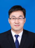 | Tao Deng Beijing Jiaotong University, China Tao Deng is a Professor and PhD Supervisor at the School of Electronic and Information Engineering, Beijing Jiaotong University. He is a recipient of the National Young Talent Program, Deputy Dean of Tianyou Zhan College, and Director of the Institute of Micro and Nano Electronics. He has led more than 10 national-level research projects, including key basic research program of the National Science and Technology Commission, pre-research funds, and National Natural Science Foundation of China projects. He has published over 90 peer-reviewed papers in prestigious journals and conferences such as Nano-Micro Letters, Advanced Functional Materials, Nano Letters, and IEEE MEMS, and owns more than 10 authorized invention patents. He has received numerous awards including the Best Researcher Award in International Sensing Technology and the Best Paper Award at IEEE NANO. Several of his developed devices have been applied in industrial applications. Speech Title: Self-Assembled 3D MEMS Sensors Abstract: As Moore’s Law approaches its physical limit, the More‑than‑Moore strategy has become essential for advanced microelectronic devices. Graphene‑based photodetectors face low absorption efficiency, while conventional two‑dimensional (2D) structures restrict device performance. This talk introduces high‑performance sensors enabled by self‑assembled three‑dimensional (3D) MEMS microtube optical resonators. The 3D architecture strongly enhances light–matter interaction, boosting responsivity by three orders of magnitude over 2D devices, with terahertz response and polarization sensitivity. Heterojunction integration with SWCNTs, TiO2, and MoS2 further improves performance, enabling self‑powered UV detection, optoelectronic synaptic functions, and polarization imaging. Inspired by spider’s mechanoreceptors, a 3D cilia‑like omnidirectional vibration transducer was developed based on flexoelectricity, delivering ultrahigh sensitivity and broad bandwidth. Combined with a 1DCNN decoupling algorithm, directional recognition reaches 97.18%. This work validates the potential of self‑assembled 3D MEMS for high‑sensitivity sensing and future integrated applications. |
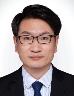 | Zhihong Liu Xidian University, China Zhihong Liu is a full Professor at the School of Microelectronics and the Guangzhou Institute of Technology, Xidian Unviersity. He is a Senior Member of IEEE. He received his B.S. and M.S. degrees from Nankai University and the Institute of Semiconductors, Chinese Academy of Sciences, respectively, and his Ph.D. from Nanyang Technological University (NTU), Singapore. In 2007, he joined Temasek Lab (TL) at NTU as a Research Associate, where he worked on the R&D of GaN microwave devices and MMIC fabrication technologies. In 2011, he joined the Singapore-MIT Alliance for Research and Technology (SMART) as Postdoc Associate, later severing as Research Scientist and Principal Research Scientist, focusing on GaN microwave/mm-wave/THz devices, GaN–Si CMOS heterogeneous integration technologies, and GaN power electronic devices. He joined Xidian University, China as a full Professor in 2019. From 2020-2025, he served as the founder and Executive Director of the Guangzhou Wide-Bandgap Semiconductor Innovation Center (GWSIC) at Xidian University. His current research interests include wide-bandgap and ultra-wide-bandgap semiconductor electronic devices and integrated circuits, with a particular focus on advanced GaN-based technologies. Speech Title: Progress of GaN-on-Si RF Devices Abstract: As a wide-bandgap semiconductor, GaN offers broad application prospects in RF fields such as radar, satellite, and 5G/6G communications. Benefiting from the advantages of GaN-based semiconductors, including a high critical electric field, high 2DEG concentration, high electron mobility, and high saturation velocity, GaN electronic devices and integrated circuits (ICs) possess excellent characteristics such as high output power, high efficiency, high-temperature operation ability etc. GaN grown a Si substrate, so called GaN-on-Si, combines the performance of GaN and the advantages of Si substrates, offering low cost, large-wafer availability, and the potential for mass production. In this talk, we will provide an overview of our recent research progress in GaN-on-Si RF devices and MMICs. Key topics include fabrication technology for 6-inch wafer C-to-Ka band GaN-on-Si device and MMICs, GaN mm-wave and THz power and low-noise transistors, and low-voltage GaN-on-Si RF devices for mobile terminal applications. |
 | Cheng Zhuo Zhejiang University, China Dr. Cheng Zhuo is a Qiushi Distinguished Professor at Zhejiang University and Vice Dean of the College of Integrated Circuits. His research interests include VLSI design, electronic design automation (EDA), and AI algorithms and systems. He has published over 200 papers in leading conferences and journals in these areas, earning five Best Paper Awards and seven Best Paper Award nominations. He currently serves or has previously served as an associate editor for journals including IEEE TCAD, ACM TODEAS, and Elsevier Integration, and has served as Chair of the ACM SIGDA East China Chapter. He has also received the First Prize of the Zhejiang Provincial Science and Technology Progress Award and the First Prize of the Zhejiang Provincial Teaching Achievement Award, among other honors. Speech Title: AI-Driven Virtual Fabrication for ICs Abstract: Amid steadily increasing process complexity and rapidly rising R&D costs, IC fabrication faces major challenges, including long development cycles and costly trial-and-error. Traditional methodologies and infrastructure struggle to support rapid iteration and fast-paced innovation. AI-driven virtual fabrication is emerging as a promising pathway to accelerate IC R&D and enhance process optimization. This report outlines key research challenges and highlights practical efforts in virtual fabrication for ICs. |
 | Yuanyuan Shi University of Science and Technology of China, China Dr. Yuanyuan Shi currently works at University of Science and Technology of China (USTC) as a professor in the school of Integrated Circuits. Before joining in USTC, she was a senior researcher at IMEC, Belgium. She received her Ph.D. degree (with Excellent “Cum Laude” Honor and Extraordinary PhD prize) from University of Barcelona in 2018. Her research interests focus on 2D and oxide semiconductors based thin-film transistors for logic, memory and brain-inspired computing. Dr. Shi has published more than 70 research articles (including Nature Electronics, IEDM, VLSI, ACS Nano, etc.), two book chapters and five international patents, etc. She served as a committee member for IEEE EDS Nanotechnology committee and several IEEE flagship conferences, including IRPS, EDTM and IPFA. Dr. Shi also serves as an active reviewer for Nature, Nature Electronics, Nature Materials, Nature Communication, ACS Nano, IEEE Electron Device Letters, and others. Dr. Shi is a recipient of Marie Skłodowska-Curie Individual Fellowship (European Commission), IEEE EDS PhD student fellowship (three winners globally each year), ADF-The Rising Stars Women in Engineering, Forbes 30 under 30 (Forbes), Park AFM award (Park Systems), etc. Speech Title: 2D-semiconductor transistors for advanced logic and memory devices: from channel deposition to device integration Abstract: Abundant-data computing such as big-data analytics, artificial intelligence (AI) and Internet of Things (IoT) demand extreme energy efficiency and concomitant improvement of cost performance of the electronic systems. Field-effect transistors (FETs) represent the fundamental building blocks for modern computer processors. The number of transistors in a typical microprocessor has followed a remarkable exponential growth since the 1960s, a trend known as Moore’s law. By making the device smaller, more transistors can be packed into a single chip with much improved performance and reduced cost. The continued miniaturization of silicon microelectronics has fuelled the exponential growth of the integrated circuits for over half a century. Today, as silicon transistors enter the sub-10nm technology node with increasing technical challenges, the exploration of alternative device geometries or new channel materials is ever more important for future processor chip. Atomically thin two-dimensional (2D) semiconductors have attracted tremendous interest as a new channel material that could facilitate continued transistor scaling. To benefit from continuous scaling, the performance of the scaled 2D transistors needs to outperform Si technology nowadays. However, significant efforts are still required for channel material deposition, gate stack development and CMOS integration, etc. This talk will present our recent progress on 2D semiconductors based logic and memory devices, including selective-area deposition of high-quality channel, scaled-device integration and 2T0C DRAM application etc. |
 | Ye LuFudan University, China Dr. Ye Lu obtained his Ph.D. from the University of Pennsylvania in 2011, and he had been with Intel and Qualcomm from 2011-2019. Dr. Lu joined Fudan University as a faculty member in early 2020, and his current research interest includes device and design co-optimization (DTCO) and AI-EDA. Dr. Lu is also a co-founder of RFIC-GPT. Speech Title: AI-Empowered Device Compact Model Creation Abstract: Device Compact Model (DCM) is a key bridge between device / process technology and circuit design simulations. Traditionally, DCM is created by physics-based formulas with human extracted parameters, however, this method is labor intensive and time consuming. This talk will cover our recent advancements in creating DCM using AI techniques such as neural networks and symbolic regression. In addition, the methodology of extracting DCM parameters using reinforcement learning (RL) will also be discussed. These results are expected to promote the efficiency as well as accuracy of future DCM development, and facilitate rapid DTCO cycles. |
 | Chunlei WuFudan University, China Prof. Chunlei Wu is an Associate Professor with the School of Microelectronics, Fudan University. Her research interests include in the area of post-Moore emerging logic devices, focusing on advanced Gate-All-Around FET, Complementary FET, etc. She has authored/co-authored more than 60 technical papers in international journals and conferences, held 16 granted patents. Speech Title: Physical Modeling of the Subthreshold Swing Saturation Behavior in Cryogenic MOSFETs Abstract: Accurate device modeling is crucial to cryogenic CMOS technology development for future quantum computing applications. The existing band tail-based models, however, arbitrarily assume an unchanged band tail states distribution at deep cryogenic temperature, resulting in significant modeling error of the subthreshold swing (SS) saturation behavior in cryogenic MOSFET. In this work, a novel band tail model featuring a temperature-dependent band tail states distribution has been presented and verified. The introduction of temperature sensitive distribution of tail states enables accurate modeling of the SS saturation value and the critical temperature corresponding to SS deviation. The results provide a deeper insight into the physical mechanisms study and modeling of cryogenic MOSFETs. |
 | Kan-Hao XueHuazhong University of Science and Technology, China Kan-Hao Xue is a professor at School of Integrated Circuits, Huazhong University of Science and Technology. He received his Bachelor's degree from the Department of Electronic Engineering, Tsinghua University, and his Master's degree from the Institute of Microelectronics, Tsinghua University, where he was honored as an Outstanding Master’s Graduate of Tsinghua University in 2007. From 2007 to 2010, he pursued his Ph.D. at the University of Colorado Colorado Springs, under the supervision of Professor Carlos A. Paz de Araujo. He has published over 170 papers in international journals. He has been listed as an Elsevier top 2% most-cited scientist worldwide. In 2018, he proposed a density functional theory-based band structure calculation method called shell DFT-1/2, which has been adopted by Synopsys in its QuantumATK simulation software. This method primarily addresses the inaccuracy of density functional theory in calculating semiconductor band gaps and extends the DFT-1/2 approach to achieve good performance for covalent semiconductors as well. In 2023, he proposed the seven-coordination theory for the origin of hafnium-based ferroelectricity. In 2024, he proposed a brand-new classification method for inorganic ferroelectric materials. In 2025, he proposed the occ DFT-1/2 method suitable for the electronic structure calculation of two-dimensional materials. Speech Title: On the direct bandgap of GaN and indirect bandgap of GaP Abstract: The direct band gap feature of GaN seems at first glance not very crucial for its power electronics applications. Yet, in case its conduction band minimum falls along the Gamma-X line like Si or Ge, it will possess much lower electron mobility. The 3d electron shell of Ga has proven significant to the direct gap feature since it pushes up the zone boundary energy eigenvalues much heavier than the zone center, through p-d repulsion, for the conduction band. Nevertheless, it is still difficult to understand the fact that both GaN and GaAs show direct bandgap while GaP suffers from an indirect gap. In this talk, we show that the direct gap feature of GaN is related to strong Coulomb attraction from the N nucleus, exerting on the conduction band electron. It is the covalent bonding feature that allows for such electron to emerge, with a nonnegligible probability, in the 2p orbital of N. In contrast, the 3p orbital of P is much farther from the nucleus, which fails to convert GaP into a direct gap semiconductor. The self-energy potential, which stems from the DFT-1/2 method, has been used to hypothetically perturb the electronegativity of elements, thus revealing the mechanism in a more vivid manner. |
 | Jiuren ZhouXidian University, China Jiuren Zhou is a Professor and Ph.D. Supervisor at Xidian University. He has been selected for China’s National Young Talent Program, recognized as a Xiaomi Young Scholar, and certified as a Category-B High-Level Talent of Hangzhou. He received his B.Eng. and Ph.D. degrees from Xidian University under the supervision of Academician Yue Hao. During his doctoral training, he conducted joint research at the University of California, Berkeley, working with Prof. Sayeef Salahuddin and Prof. Chenming Hu, and later carried out research at the Silicon Nano Device Laboratory (SNDL) of the National University of Singapore. He is currently a core member of the research team led by Academician Yue Hao and Prof. Genquan Han at the Hangzhou Institute of Xidian University. His research focuses on emerging ferroelectric memories, in-memory computing devices, and advanced computing chips. He has published over 100 papers in leading microelectronics journals and conferences, including IEEE IEDM, VLSI, EDL, and TED. He authored the monograph Negative Capacitance Field-Effect Transistors and holds more than 30 invention patents. He has led three national-level research projects, including a sub-project of the Science and Technology Innovation 2030 Program, and has received multiple academic honors. Speech Title: >1010-Cycle Endurance in Wurtzite Ferroelectrics via a Superlattice and Recovery Protocol Enabling Vacancy Confinement Abstract: Wurtzite-structured ferroelectrics offer distinct advantages for ultra-high-density, large-scale integrated memory due to their quasi-single-crystalline three-dimensional lattice architecture. However, their application is fundamentally constrained by endurance degradation under electrical cycling, with fatigue failure typically occurring before 108 cycles. The underlying microscopic mechanisms remain poorly understood. Here, we identify nitrogen vacancy (VN) clustering and long-range vertical migration as primary contributors to endurance breakdown. To address this, we design a spatially engineered AlScN/AlN superlattice coupled with a dynamic recovery protocol, jointly suppressing VN accumulation and mobility in both spatial and energetic domains. This combined approach stabilizes the defect distribution under high-field cycling, mitigating dielectric breakdown and polarization degradation. Consequently, we demonstrate ferroelectric endurance exceeding 1010 cycles in a wurtzite system—surpassing prior records by two orders of magnitude. This work clarifies the fatigue-inducing role of VN and establishes a structural–defect co-engineering strategy for highly reliable ferroelectric devices. |
 | Dexing LiuThe Chinese University of Hong Kong, Shenzhen, China Dr. Dexing Liu obtained his B.S. in Applied Physics from Shandong University in 2020 and earned his Ph.D. in Integrated Circuit Science and Engineering from Peking University in 2025. In 2024, he was a visiting scholar in the Department of Applied Physics at The Hong Kong Polytechnic University. He is currently a postdoctoral fellow at The Chinese University of Hong Kong, Shenzhen. His research focuses on semiconductor device physics, post-Moore era electronic devices, and design-technology co-optimization. To date, he has published nearly ten (co-)first-author papers in journals such as Nature Nanotechnology and Advanced Materials, with over 20 SCI publications and more than 400 citations. He has received multiple awards, including the National Scholarship, Beijing Outstanding Graduate, Peking University Outstanding Graduate, Baidu ERNIE Science and Technology Innovation Star Award, and Shenzhen Outstanding Academic Paper Award. Speech Title: Making Efficient Electrical Contacts in Low-Dimensional Semiconductors Abstract: The performance of low-dimensional semiconductors, which are pivotal for post-Moore nanoelectronics, is severely limited by high contact resistance and poor metal-semiconductor interfaces. To overcome these bottlenecks, we introduce Mc4 (Making Clean, Close, Complementary Contacts), a systematic framework for atomic-level interface engineering. The multidisciplinary approach combines theoretical modeling, interface modulation, and experimental validation to achieve two key advances. First, the discovery of a quantum limit in contact resistance enabled by hydrogen-bonded, non-covalent contacts that mitigate Fermi-level pinning and contamination. Second, a flexible integration strategy producing MXene-based hydrogen-bonded heterojunctions with outstanding charge transport and durability, as evidenced by CNT transistors retaining 74 cm2 V-1 s-1 mobility after 100,000 bending cycles. This work bridges atomic precision with scalable fabrication, offering a universal pathway toward high-performance low-dimensional flexible electronics. |
| Yancong QiaoSun Yat sen University, China Yancong Qiao is an associate professor in the School of Biomedical Engineering at Sun Yat-sen University. He received his B.S. degree from the Department of Electronic Science and Technology of Xi’an Jiaotong University in 2016 and his Ph.D. degree from the School of Integrated Circuits of Tsinghua University in 2021. His current research interests focus on flexible MEMS systems, biomedical micro/nano sensing, flexible electronic skins, and systems, soft robot, as well as, soft robots, etc. He has published more than 60 papers, including 27 as the first author and corresponding author in well-known journals such as Science Advances, Advanced Functional Materials, Nano-Micro Letter, InfoMat, ACS Nano, and has been cited more than 3500 times in Google Scholar. His h-factor is 30 and i10 factor is 40. He has been authorized the first inventor to hold 5 invention patents and lead multiple projects from the NSFC, Guangdong Province, and Shenzhen City. Speech Title: Flexible Ultra-Thin Physiological Signal Sensor and Thermal-Electric Conversion System Abstract: In recent years, flexible electronic technology has developed rapidly in the field of physiological signal monitoring. However, one important factor currently limiting the widespread application of flexible physiological signal sensors is the interface problem between the sensors and the human body. To optimize the sensor/skin interface, an effective method is realizing ultra-thin electronic skin sensor, which, on one hand, can suppress motion artifacts and improve signal quality; On the other hand, can improve the user's wearing experience, expand the amount of physiological signal database, and provide a data foundation for further integration with artificial intelligence algorithms to achieve intelligent sensors. In this report, graphene and Nanomesh is used as the core sensing materials. Laser scribing graphene is investigated to achieve device pattern and high-quality transfer technology, and multiple methods of preparing Nanomesh have been developed, based on which a series of devices such as high-sensitivity strain sensors, ultra-thin and insensitive physiological electrodes, and artificial intelligence assisted sweat sensors have been realized. Nanomesh sensors can achieve a good interface with the skin without external fixation, greatly improving the user's wearing experience. This report will also introduce flexible sensor enhancement technologies such as Nanomesh reinforcement and microcavity assistance, which greatly improve the stability, linearity, and work range of flexible mechanical sensors. Based on graphene and Nanomesh sensors, various physiological signals are collected and many databases are built. By combining with artificial intelligence algorithms, intelligent analysis and diagnosis of various physiological signals such as blood pressure, sweat output, respiration, tactile, and movement are ultimately achieved. Meanwhile, this report will also discuss the application of ultra-thin electronic skin sensors in soft robots and human-computer interaction field. |
 | Ming QiaoUniversity of Electronic Science and Technology of China, China Ming Qiao, Ph.D., Professor and Doctoral Supervisor at University of Electronic Science and Technology of China (UESTC). His research focuses on power semiconductor devices, high-voltage power integration technologies, power device reliability, radiation-hardened power devices, and power device modeling. He has received two second prize of National Science and Technology Progress Awards, five provincial and ministerial-level science and technology awards, Huawei Spark Award and so on. He has authored over 200 papers and holds 16 U.S. patents and more than 100 Chinese invention patents as the first inventor. He serves on the technical program committee of ISPSD, and on the editorial board of Microelectronics Journal. Speech Title: Customized Design of Low-Voltage LDMOS to Reduce Energy Losses for xPU Power Supply Abstract: DrMOS based on LDMOS is a key enabler for on-chip xPU power supply. To achieve high efficiency, low-side LDMOS requires low specific on-resistance (RSP) while high-side LDMOS demands low gate-charge (QG). This talk presents a suite of customized LDMOS techniques on a 55 nm BCD platform. These include CFP and short-channel process for reduced channel resistance, grid-gate layout for higher linear current, biased split gate structures for superior RSP·QGD trade-off, and timing-controlled auxiliary gate for lower switching losses. Experimental results confirm these designs are highly suitable for next-generation DrMOS application. |
 | Xuefei LiHuazhong University of Science and Technology, China Dr. Xuefei Li received his PhD from Nanjing University in 2013. He was a visiting scholar at Purdue University from November 2011 to May 2013. He is currently an associate professor at Huazhong University of Science and Technology. His research focuses on advanced logic devices based on two-dimensional semiconductors. He has published over 40 papers in prestigious international journals such as Nature Electronics, Science Advances, Advanced Materials, Nano Letters, ACS Nano, and IEEE Electron Devices Letters. He demonstrated the first negative differential resistance (NDR) effect in a MoS₂ transistor due to self-heating and developed the world's first ballistic black phosphorus field-effect transistor. Speech Title: Ballistic transport in p-type WSe2 transistors Abstract: To realize 2D CMOS logic circuits, p-type 2D transistors with comparable performance to that of nFETs are essential. WSe2 is a promising 2D p-type semiconductor due to its high intrinsic hole mobility and relatively large band gap. However, the selenium vacancy in the WSe2 film grown by CVD and the damage caused by metal contact formation can lead to undesired large Schottky barrier heights and contact resistance Rc, which severely limits the electrical performance of WSe2 pFETs, especially short-channel devices. In this work, we report an oxygen p-doping and full contact structure to reduce the contact resistance of monolayer p-type tungsten diselenide and demonstrate high-performance p-type WSe2 field-effect transistors. The controllable oxygen doping and the full contact structure greatly increase the contact quality. Consequently, short-channel WSe2 pFETs deliver a record saturation current and a ballistic ratio of 81% at room temperature. Our work presents a straightforward and versatile technique to achieve high-performance p-type two-dimensional electronics beyond silicon. |
 | Donglin LuHunan university, China Donglin Lu is an associate professor, doctoral supervisor, and Yuelu Scholar at the School of Physics and Electronics, Hunan University. He joined Hunan University as a postdoctoral researcher in 2020 and transitioned to the associate professor position in 2024. He has led projects including the Young Scientists Program C of the National Natural Science Foundation of China and a sub-project of the National Key R&D Program for Young Scientists. He has been recognized under talent programs such as the Furong Program for Scientific and Technological Innovation Young Talents in Hunan Province and the National Postdoctoral Program for Innovative Talents. His research focuses on novel semiconductor three-dimensional hetero-integration and interface regulation. He has published over 40 high-impact papers in journals such as Nature, Nature Communications, and ACS Nano, including a paper as first author in Nature. Speech Title: High-density 3D integration based on 2D semiconductors Abstract:As integrated circuit technology enters the sub-10 nm node, the practical channel length of silicon-based transistors becomes difficult to scale further, and density enhancement faces bottlenecks. Consequently, transistor integration technology is shifting from planar integration to 3D vertical integration. This report focuses on high-density 3D integration of 2D semiconductors. We propose an integrated vdW monolithic 3D integration process, in which pre-fabricated integrated vdW circuit layers and 2D semiconductor layers are stacked layer-by-layer. This approach overcomes the thermal budget limitations of monolithic 3D integration and avoids the damage to 2D semiconductors caused by traditional high-energy integration processes, achieving monolithic 3D integration of 10 circuit layers and multifunctional cooperative operation. Furthermore, we develop an exponential bisecting 3D stacking process. Planar devices on a sacrificial silicon substrate are cut in half along the midline; then one half of the device layer is separated from the substrate and bonded to the other half, forming a two-layer stacked structure. By repeating this bisecting-stacking process N times, a high-order 3D integrated system with 2N layers is ultimately realized. Using this process, we demonstrate for the first time a 1024-layer high-density 3D chip integration, achieving an integration density of 1.5 × 10⁹ Tr/mm2, representing the highest number of integrated layers and the highest integration density to date. |
 | Sunbin DengHuazhong University of Science and Technology, China Dr. Sunbin Deng received his B.Sc. degree from Huazhong University of Science and Technology (HUST), Wuhan, China, in 2014, and his Ph.D. degree in Electronic and Computer Engineering from the Hong Kong University of Science and Technology (HKUST), Hong Kong SAR, in 2020. Subsequently, he held postdoctoral fellow positions at Purdue University (2021–2022) and Georgia Institute of Technology (2022–2025). Dr. Deng is currently a Professor at the School of Optical and Electronic Information, HUST. His research focuses on back-end-of-line (BEOL)-compatible thin-film (opto-)electronics, with a particular emphasis on oxide semiconductor transistors, for monolithic 3D integration, electronic-photonic integration, alternative computing, and information display technologies. To date, Dr. Deng has co-authored 80+ publications, including 30+ papers as first or corresponding author, in leading peer-reviewed journals (e.g., Sci. Adv., Nat. Commun.) and top-tier international conferences (e.g., IEDM, VLSI). He has received several academic awards, including the Distinguished Paper Award at SID Display Week Symposium and the Young Leader Award from SID. Speech Title: BEOL-Compatible Oxide Power Transistors for On-Chip Active Power Delivery Networks in 3D ICs Abstract: Increasing power demands and the presence of multiple supply voltage domains pose unprecedented challenges for power delivery in 3D integrated circuits (ICs). Distributing integrated voltage regulators (IVRs) throughout 3D ICs to realize active power delivery networks (PDNs) offers a scalable and energy-efficient solution. In this talk, I will introduce back-end-of-line (BEOL)-compatible amorphous oxide semiconductor (AOS) power transistors as a competitive active device technology for on-chip voltage conversion. Significant recent advances in AOS materials, device structures, and fabrication processes have substantially improved transistor performance and reliability. As a result, ITO planar power transistors with a specific on-resistance (Ron,sp) as low as 87 mΩ·mm² have enabled the experimental demonstration of switched-capacitor DC-DC converters, which achieved a stage efficiency of ≥87.5% for 2:1 step-down conversion from 12 V. Furthermore, by developing IGO vertical power transistors with an ultralow Ron,sp of 0.04 mΩ·mm², the converters operating at a 3 V voltage rating could achieve a simulated peak stage efficiency of 94.3%. These results highlight the great potential of AOS power transistors for enabling highly efficient IVRs and, ultimately, active PDNs in 3D ICs. |
 | Daquan ZhangSchool of Science and Engineering, The Chinese University of Hong Kong (Shenzhen), China Dr. Daquan Zhang is an Assistant Professor in the School of Science and Engineering at The Chinese University of Hong Kong, Shenzhen. He earned his B.Eng. degree and Ph.D. degree from Wuhan University in 2014 and HKUST in 2020, respectively. After that, he worked as a Research Associate and Research Assistant Professor at HKUST from 2020 to 2024. His research focus is on the growth and carrier dynamics study of metal halide perovskite nanomaterials and their applications in high-performance optoelectronic devices. He has published over 50 journal articles, with first-/corresponding-author papers in Nature Photonics, Advanced Materials, Nano Letters, NPJ Flexible Electronics, etc. Speech Title: Metal halide perovskite nanowire arrays for high-performance optoelectronic devices Abstract: Metal halide perovskite (MHP) nanowires (NWs) have energized remarkable research interests owing to their unique characteristics of grain-boundary-free, efficient axial carrier transportation, and strong radial spatial-confinement. However, low photoluminescence quantum yield (PLQY) is usually achieved in MHP NWs because of severe surface non-radiative recombination, which limits their applications in high-performance optoelectronics, such as photodetectors (PDs), solar cells, lasers and light-emitting diodes (LEDs). Here, vertically aligned, high-quality and ultrahigh-density MHP NW arrays have been fabricated in porous alumina membranes with vapor-phase and solution-phase strategies. The obtained MHP NWs possess significantly high (>90%) PLQY and excellent chemical stability. The fabrication is also compatible with large-scale rigid and flexible substrates. Consequently, they have been fabricated into high-performance and flexible optoelectronic devices, including LEDs, narrowband and self-powered PDs, etc. These results suggest that the MHP NWs are highly promising to broaden the development of MHP nanomaterials and promote their practical applications in high-performance optoelectronics. |


